In the wireless digital communication, it is ------ to transmit the digital data directly
good
easy
bad
not easy
In digital communication, it needs to pass through the modulator and modulate the ----- signal in order to send the signal effectively
analog
carrier
digital
actual
In the wireless digital communication, when we modulate the amplitude of the carrier this kind of modulation is called -------
PCM
FSK
ASK
PSK
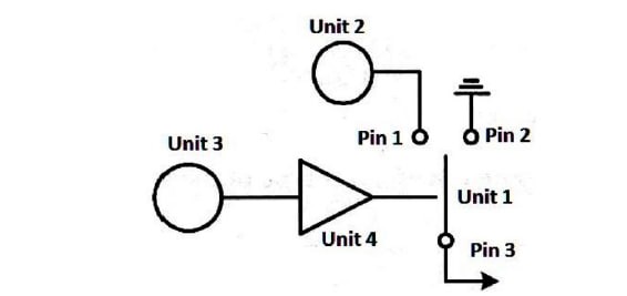
Figure (1) shows the basic block diagram of ------- modulator.
FSK
ASK
PSK
PCM
In the basic block diagram shown if Figure (1), Unit 3 is represents --------
information
carrier signal
digital signal
analog signal
In the basic block diagram shown if Figure (1), Unit 2 is represents --------
digital signal
analog signal
information
carrier signal
In the basic block diagram shown if Figure (1), Unit 4 is represents --------
buffer
analog signal
switch
carrier signal
In the basic block diagram shown if Figure (1), Unit 1 is represents --------
analog signal
switch
buffer
information
In the basic block diagram shown if Figure (1), the output signal is taken from -----
Pin 1
Pin 2
Pin 3
Pin 1 or Pin 2
In Figure (1), when the data input is high, the output signal is coming from -------
Pin 2
Pin 1
Pin 3
Pin 1 or Pin 2
In Figure (1), when the data input is low, the output signal is coming from -------
Pin 2
Pin 1
Pin 3
Pin 1 and Pin 2
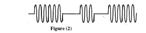
The waveform shown in Figure (2) is the output of the ------- modulator.
PCM
ASK
FSK
PSK
The digital data used to produce the modulate waveform shown in Figure (2) is ------
1001011
1100011
1101011
1101001
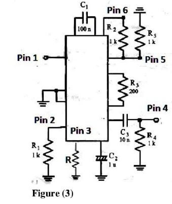
The circuit diagram shown in Figure (3) is used to implement ------- modulator.
FSK
PCM
PSK
ASK
The circuit diagram shown in Figure (3), resistors ------- comprise a voltage divided circuit.
R2, R3
R2 R5
R2, R4
R1, R3
In Figure (3), the main fun
offset
positive
composite
negative
In Figure (3), the first oscillation frequency is determined by resistor ------
R1
R2
R3
R4
In Figure (3), the first oscillation frequency is determined by resistor connected at -----
-
Pin1
Pin2
Pin3
Pin4
In Figure (3), the second oscillation frequency is determined by resistor ------
R1
R2
R3
R
In Figure (3), the second oscillation frequency is determined by resistor connected at ------
Pin 5
Pin 4
Pin 3
Pin 6
In Figure (3), the digital data is inputted at -------
Pin 4
Pin 3
Pin 1
Pin 2
In Figure (3), the DC power supply is inputted at -------
Pin 5
Pin 6
Pin 4
Pin 3
In Figure (3), the second oscillation frequency is equal to zero when ------is opened.
Pin 6
Pin 4
Pin 5
Pin 3
In Figure (3), the output modulated signal is taken from -----
Pin 6
Pin 5
Pin 4
Pin 2
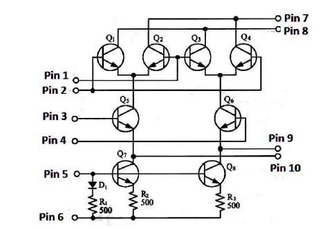
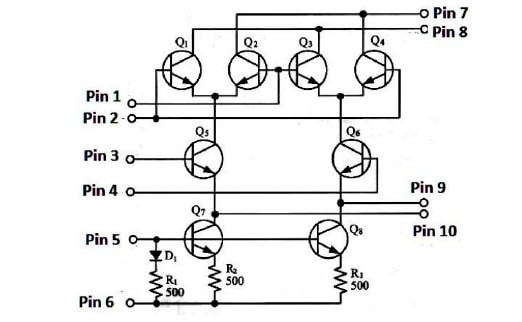
In the circuit diagram shown in Figure (4), the elements D1, R1, R2, R3, Q7 and Q8 comprise a -------
dc voltage source
dc current source
ac current source
ac voltage source
In the circuit diagram shown in Figure (4), the elements D1, R1, R2, R3, Q7 and Q8 comprise ------- to Q5 and Q6.
dc bias voltage
ac bias current
dc bias curren
ac bias voltage
In the circuit diagram shown in Figure (4), the Q5 and Q6 comprise a ------- amplifier
differential
difference
summing
summer
In the circuit diagram shown in Figure (4), the dc bias of Q1, Q2, Q3, and Q4 are ------
Q5 and Q7
Q5 and Q8
Q5and Q6
Q8 and Q7
In the circuit diagram shown in Figure (4), the data signal is inputted between -----.
Pin1 and Pin 2
Pin3 and Pin 4
Pin5 and Pin 6
Pin7 and Pin 8
In the circuit diagram shown in Figure (4), The carrier signal is inputted between ------
Pin1 and Pin 2
Pin3 and Pin 4
Pin5 and Pin 6
Pin9 and Pin 10
In the circuit diagram shown in Figure (4), the gain of balanced modulator is inputted between -----
Pin3 and Pin 4
Pin5 and Pin 6
Pin7 and Pin 8
Pin9 and Pin 10
In the circuit diagram shown in Figure (4), the bias adjustment is inputted between -----
Pin3 and Pin 4
Pin5 and Pin 6
Pin7 and Pin 8
Pin9 and Pin 10
The circuit diagram shown in Figure (4) is called -------modulator.
synchronous
unbalanced
asynchronous
balanced
In digital communication systems, we need a----- to modulate the data to a high carrier frequency
decoder
modulator
demodulator
encoder
In digital communication systems, the main function of the receiver is to convert the digital signal back to the ------ signal.
encoded
modulated
decoded
modulating
In digital communication systems, there are ------ methods to design the ASK demodulator.
few
many
two
three
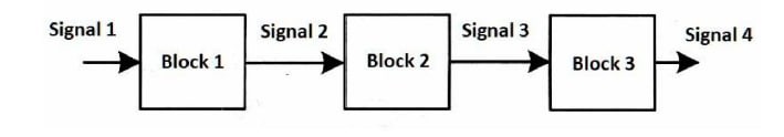
In the block diagram shown in Figure (1), Signal 1 is called ---------- ASK signal.
analog
modulating
data
modulated
In the block diagram shown in Figure (1), Block 1 is called -------
rectifier
LPF
comparator
HPF
In the block diagram shown in Figure (1), Block 2 is called -------
comparator
HPF
LPF
rectifier
In the block diagram shown in Figure (1), Block 3 is called -------
HPF
comparator
rectifier
LPF
In the block diagram shown in Figure (1), Signal 2 is called ----- signal
amplified
filtered
compared
rectified
In the block diagram shown in Figure (1), Signal 3 is called ----- signal
filtered
rectified
amplified
compared
In the block diagram shown in Figure (1), Signal 4 is called ----- signal
amplified
modulating
filtered
rectified
When ASK signal pass through the------ we can obtain the positive half wave signal.
HPF
LPF
comparator
rectifier
When the rectified ASK signal pass through the------ we can obtain an envelop detection.
LPF
comparator
rectifier
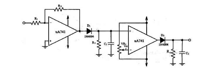
Figure (2), shows the circuit diagram of ------- ASK detector
synchronous
digital
asynchronous
analog
In Figure (2), R1, R2 and μA741 comprise an -------
rectifier
non inverting amplifier
LPF
inverting amplifier
In Figure (2), D1 is the ------- diode.
rectifying
voltage regulator
varactor
full wave rectifier
In digital communication systems, we need a modulator to modulate the data to a high ----- frequency.
analog
signal
carrier
digital
In Figure (2), R3 and C1 comprise ------- filter
a high pass
a low-pass
a band pass
a band stop
In Figure (2), μA741, VR1, D2, R4, and C2 comprise -------
a comparator
LPF
rectifier
amplifier
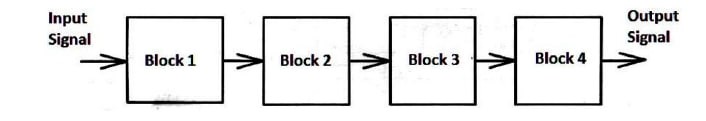
For the block diagram shown in Figure (3), its input signal is called ------ signal.
analog
modulated
modulating
information
For the block diagram shown in Figure (3), Block 1 is called ------
comparator
LPF
voltage limiter
square law detector
For the block diagram shown in Figure (3), Block 2 is called ------
LPF
voltage limiter
square law detector
comparator
For the block diagram shown in Figure (3), Block 3 is called ------
square law detector
comparator
LPF
voltage limiter
For the block diagram shown in Figure (3), Block 4 is called ------
comparator
LPF
voltage limiter
square law detector
In the circuit diagram shown in Figure (4), the elements D1, R1, R2, R3, Q7 and Q8comprise a -------
dc voltage source
dc current source
ac current source
ac voltage source
In the circuit diagram shown in Figure (4), the elements D1, R1, R2, R3, Q7 and Q8comprise ------- to Q5 and Q6.
dc bias voltage
ac bias current
dc bias current
ac bias voltage
In the circuit diagram shown in Figure (4), the Q5 and Q6 comprise a ------- amplifier
differential
difference
summing
summer
In the circuit diagram shown in Figure (4), the dc bias of Q1, Q2, Q3, and Q4 are ------
Q5 and Q7
Q5 and Q8
Q5and Q6
Q8 and Q7
In the circuit diagram shown in Figure (4), the data signal is inputted between -----.
Pin1 and Pin 2
Pin3 and Pin 4
Pin5 and Pin 6
Pin7 and Pin 8
In the circuit diagram shown in Figure (4), The carrier signal is inputted between ------
Pin1 and Pin 2
Pin3 and Pin 4
Pin5 and Pin 6
Pin9 and Pin 10
In the circuit diagram shown in Figure (4), the gain of balanced modulator is inputted between -----
Pin3 and Pin 4
Pin5 and Pin 6
Pin7 and Pin 8
Pin9 and Pin 10
In the circuit diagram shown in Figure (4), the bias adjustment is inputted between -----
Pin3 and Pin 4
Pin5 and Pin 6
Pin7 and Pin 8
Pin9 and Pin 10
The circuit diagram shown in Figure (4) is called -------modulator.
synchronous
unbalanced
asynchronous
balanced
{"name":"In the wireless digital communication, it is ------ to transmit the digital data directly", "url":"https://www.quiz-maker.com/Q7D8PX3ZS","txt":"In the wireless digital communication, it is ------ to transmit the digital data directly, In digital communication, it needs to pass through the modulator and modulate the ----- signal in order to send the signal effectively, In the wireless digital communication, when we modulate the amplitude of the carrier this kind of modulation is called -------","img":"https://www.quiz-maker.com/3012/images/ogquiz.png"}