ELEX SYSTEM AND DESIGN-ECE3C

ELEX System and Design Quiz
Welcome to the ELEX System and Design Quiz, designed to test your knowledge and understanding of various electronic concepts. With 90 thought-provoking questions, this quiz challenges your grasp of MOSFETs, JFETs, biasing techniques, and transistor operations.
Enhance your learning experience and see how well you can answer questions like:
- What determines the characteristics of MOSFETs?
- In which region of operation does the collector of a transistor act like a current source?
- How many terminals are there in a MOSFET?
The drain current n-MOSFET is varied by
Gate to Source voltage
Gate current
Source Voltage
None of the above
A mosfet's output characteristics is plot of
ID as a function of VDS with VGS as a parameter
Ig as a function of Vds with Vgs as a parameter
Id as a function of Vgs with Vds as a parameter
Ig as a function of Vgs with Vds as a parameter
Region where MOSFETs operate as amplifiers
Saturation region
Cutoff region
Triode/linear region
None
Which of the following terminals is not a part of the MOSFET?
Gate
Base
Source
Drain
The MOSFET stands for _
Metal oxide surface FET
Metal of surface FET
Metal Oxide Semiconductor FET
Metal oxidized selenium FET
How many terminals are there in a MOSFET?
3
4
2
16
The layer that separates the Gate terminal from the semiconductor is
Silicon
Silicon Oxide
Silica
Silicon dioxide
The one referred to as an open switch
Depletion mosfet
UJT
JFET
Enhancement MOSFET
What determines the characteristics of MOSFETs?
Enhancement type
Depletion type
A and b
None of the above
This type of FET is usually referred to as ON Switches.
Depletion MOSFET
JFET
MOSFET
Enhancement MOSFET
A transistor operating in the active region has a base current, IB, of 20µA. If β = 250, how much is the collector current, IC?
50mA
5mA
12.5ma
80ua
When a transistor is in saturation,
VCE = VCC
IC = 0 A
VCE = 0 V
VCE = 1/2 VCC
A transistor has a collector current, IC, of 10 mA. How much is the base current, IB if the transistor has a βDC of 50, 100, 200, and 250 respectively?
200µA, 100µA, 50µA, 40µA
200µA, 100µA, 50µA, 20µA
200µA, 100µA, 40µA, 20µA
2000µA, 50µA, 40µA, 20µA
In what region of operation does the collector of a transistor act like a current source?
The cutoff region
The active region
The saturation region
None of the above
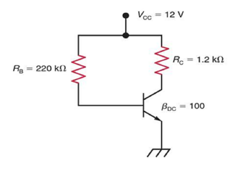
Fig1. What form of bias is shown?
Fixed Bias or Base bias
Emitter Bias
Voltage Divider Bias
Collector Feedback Bias

In Fig. 1, solve for the following IB and IC.
IB = 61.4µA and IC = 6.14mA
IB = 41.4µA and IC = 4.14mA
IB = 51.4µA and IC = 5.14mA
IB = 51.4µA and IC = 5.14µA
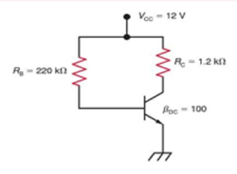
In Fig. 1, solve for the following VCE and IC (sat)
VCE = 6.83V and IC(sat) = 10mA
VCE = 5.83V and IC(sat) = 20mA
VCE = 5.83V and IC(sat) = 10µA
VCE = 5.83V and IC(sat) = 10mA

In Fig. 1, Find VCE(off)
10V
8V
12V
14V

What form of bias is shown in Fig. 2?
A. Fixed Bias or Base bias
Emitter Bias
Voltage Divider Bias
Collector Feedback Bias
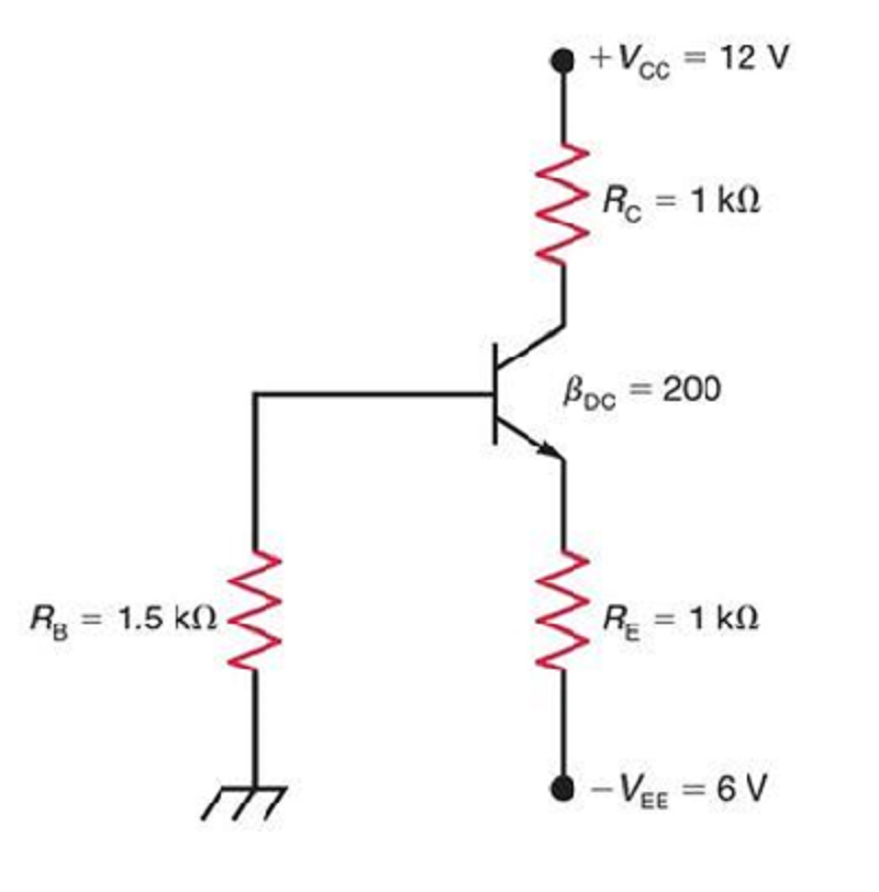
In Fig. 2, solve for IE and VC
IE = 5.3mA and VC = 6.7V
IE = 6.3mA and VC = 6.7V
IE = 5.3mA and VC = 5.7V
IE = 6.3A and VC = 6.7V
Which of the following statements are true?P: JFET is biased to operate it in active region Q: MOSFET is biased to operate it in saturation region
Both P and Q are correct
P is correct and Q is incorrect
P is incorrect and Q is correct
Both P and Q are incorrect
A p-channel JFET requires a
Negative gate to source voltage
Negative drain to source voltage
Positive drain to source voltage
Positive gate to source voltage
Most common type of JFET biasing is
Current biasing
Voltage biasing
Self-biasing
None of the above
In a certain self-biased n-channel JFET circuit, if drain current is equals to 2mA and source resistance is equals to 1.0kΩ then gate to source voltage is equals to?
8mV
-3V
-2V
2V
In a JFET, the level of ________ is limited to values between 0 V and –VP.
VGSQ
VDSQ
VDGQ
VSQ
Which of the following is true?
JFETS are normally closed devices
JFETS are normally open devices
A and B are both true
None of the above
If an N-channel JFET with voltage divider bias has a gate voltage of 7V and source voltage of 8V then the gate to source voltage would be ___.
1V
2V
-2V
-1V
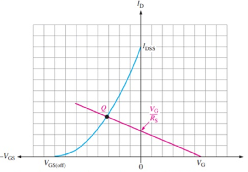
What type of biasing is represented by the image below?
Fixed Bias
Self-Bias
Voltage Divider Bias
None of the above
All are the operating regions of a JFET except
Cut-off region
Saturation Region
Breakover region
Ohmic Region
It is a technique used to increase Q point stability of self-biased junction field-effect transistor through making ID independent on the VGS.
Self-Bias
Q-point Bias
Voltage Divider Bias
Current-source Bias
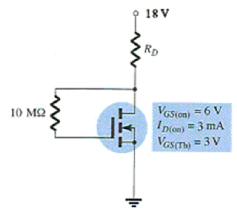
Calculate the value of Rd
4.13 kΩ
3 kΩ
2kΩ
3.5 kΩ
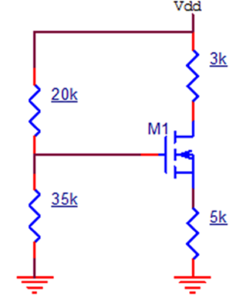
Consider the following circuit. Process transconductance parameter = 0.50 mA/V2, W/L=1, Threshold voltage = 3V, VDD = 20V. Find the operating point of circuit
20V, 23.61mA
12.72V, 23.61mA
13V, 22mA
20V, 25mA
For a MOSFET, the pinch-off voltage is -3V. Gate to source voltage is 20V. W/L ratio is 5. Process transconductance parameter is 40μA/V2. Find drain to source current in saturation.
0.10 mA
� 0.05mA
0.05mA
� 50A
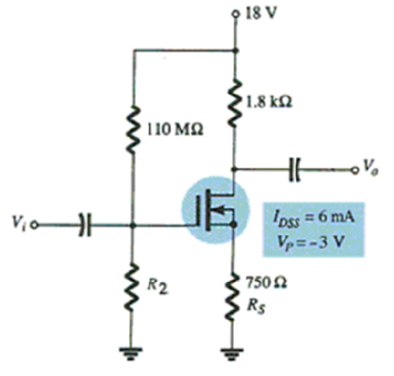
For what value of R2 is VGSQ equal to 1 V?
10 MΩ
100 MΩ
220 MΩ
110 MΩ
For an n-channel E-MOSFET with gate to source voltage equals to 2V, gate to source voltage to conduct must exceeds
2V
4V
1V
6V
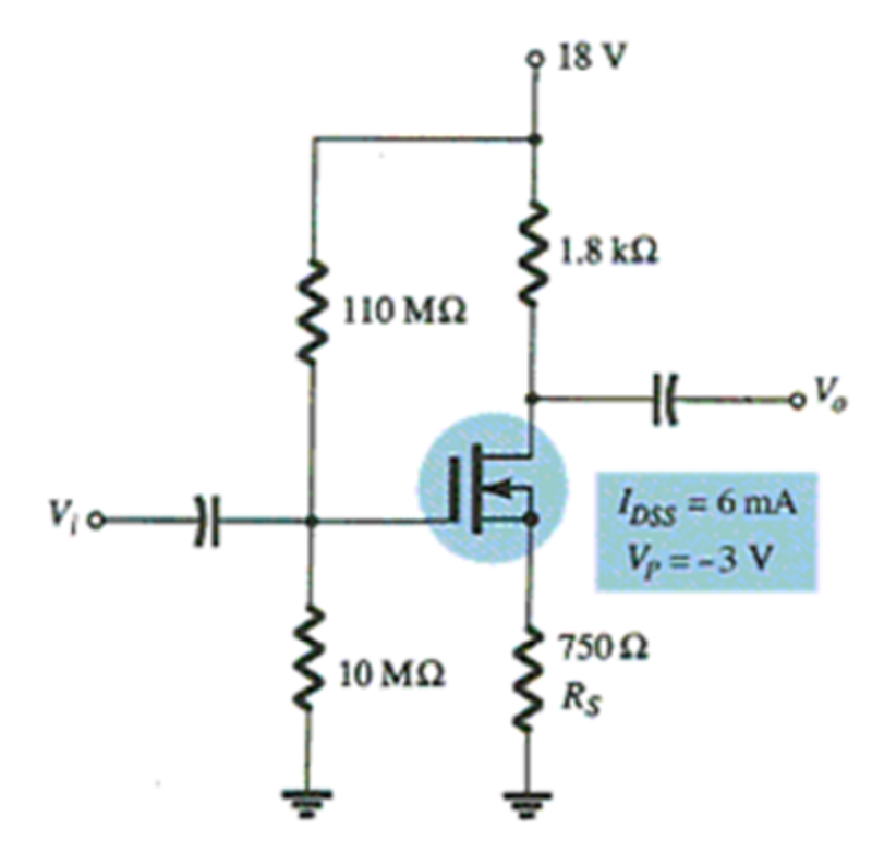
At what value of RS does the circuit switch from depletion mode to enhancement mode?
250 Ω
500 Ω
10 MΩ
None of the above
For an n-channel e-mosfet Vth=5V, what is the condition to turn on the device
Vds>5V
Vgs>5V
Vgs<5V
Vds=5V
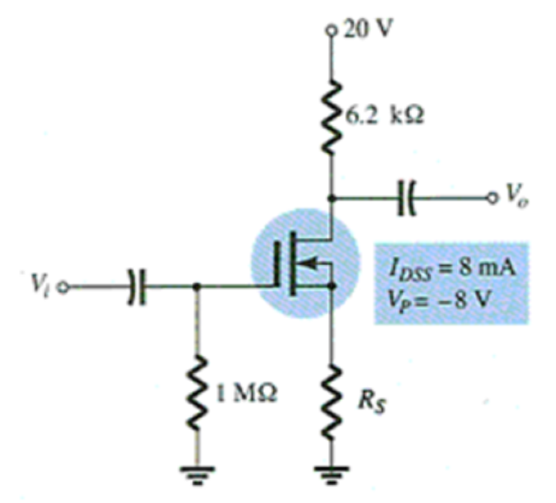
For what value of RS can the depletion-type MOSFETs operate in enhancement mode?
None of the above
5 kΩ
2.4 kΩ
6.2 kΩ
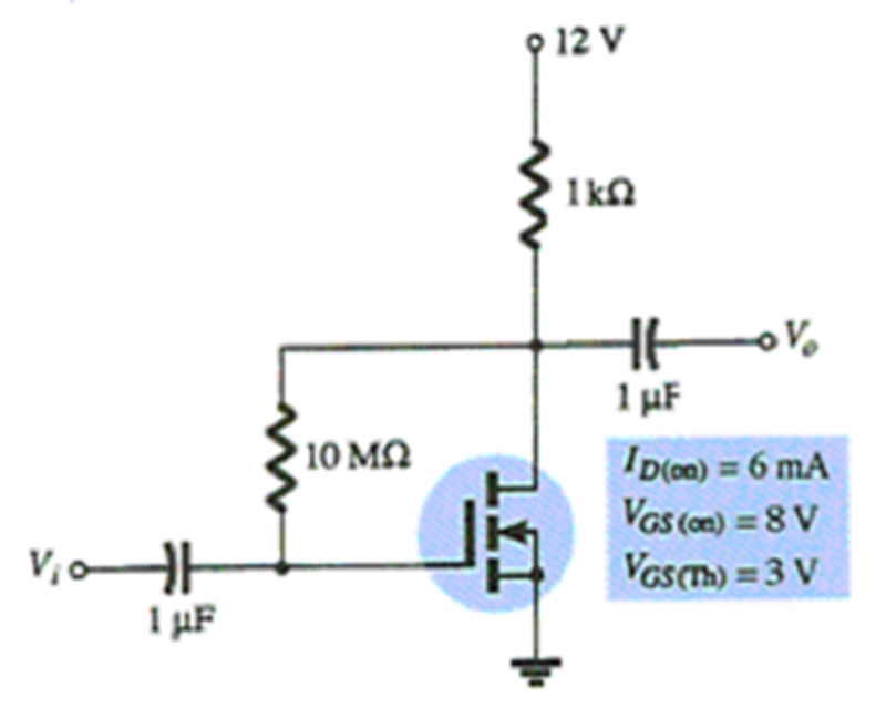
Determine the value of VDSQ.
3.5 V
4.86V
7.14V
10 V
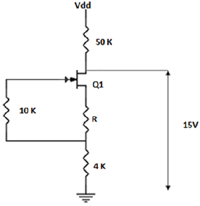
Consider the following circuit. IDSS = 2mA, VDD = 30V. Find R, given that VP = – 2V.
10kΩ
2kΩ
4kΩ
5kΩ
The three basic op-amp configurations are _________.
Inverting, noninverting, and voltage follower
Base, emitter, collector
Drain, source, gate
D. inverting, gate, current follower
It is the total resistance between the inverting and the non-inverting inputs.
Common-mode input impedance
Differential input impedance
Input offset voltage drift
Slew rate
Two types of op-amp input operation are the ________.
Differential mode and the common mode
n-type and p-type
Electron and holes
Inverting and noninverting
It provides amplification of the difference voltage between the two inputs.
Class A Differential Amplifier
Differential Amplifier
Push-pull class B amplifier
Push-pull amplifier
It has the highest input impedance and the lowest output impedance of the three amplifier configurations.
Voltage-follower
Inverting
Non-inverting
Common mode
A noninverting amplifier configuration has a _____________ than the op-amp itself (without feedback).
Lower input impedance and a higher output impedance
Higher input impedance and a higher output impedance
Lower input impedance and a lower output impedance
Higher input impedance and a lower output impedance
It is an Op-Amp parameter which is the gain of the op-amp without positive or negative feedback.
Bandwidth
Open Loop Gain
Output impedance
Input Impedance
It is the frequency range over which the voltage gain of the amplifier is above 70.7% or -3dB of its maximum output.
Bandwidth
Offset Voltage
Voltage Gain
Closed Loop Gain
It is a process of “feeding back” a fraction of the output signal back to the input, and feeding it back to the negative terminal using external feedback resistor.
Positive Feedback
Negative Feedback
Virtual Earth
Neutral Feedback
An amplifier circuit which converts current generated by the photo-diode into a voltage
Inverting Operational Amplifier
Voltage Follower
Trans-resistance Amplifier Circuit
Non-Inverting Operational Amplifier
A certain op-amp has an open-loop differential voltage gain of 25,000 and a common-mode gain of 0.2. Determine the CMRR in decibels.
102 dB
114 dB
98 dB
122 dB
It is the ability of an amplifier to reject common-mode signals is a parameter called the ?
CRMR
CMRR
CMRS
DMRS
At low frequencies, this noise in an Op-Amp is inversely proportional to the frequency is called?
Pink Noise
White Noise
Low Noise
Overpass Noise
The internal amplifier stages that make up an op-amp have voltage gains limited by?
Internal resistance
Junction capacitance
Both of the above
None of the above
In an Op-Amp the input offset current equals the .
Average of two base currents
Collector current divided by the current gain
Sum between two base-emitter voltages
Difference between two base currents
A series dissipative regulator is an example of a:
Shunt Regulator
Dc-to-dc converter
Linear Regulator
Switching regulator
The usefulness of an op-amp operated without negative feedback is generally limited to comparator applications. With negative feedback, the closed-loop voltage gain (Acl) can be reduced and controlled so that the op-amp can function as a _______.
Linear amplifier
Power amplifier
Current Amplifier
Voltage Amplifier
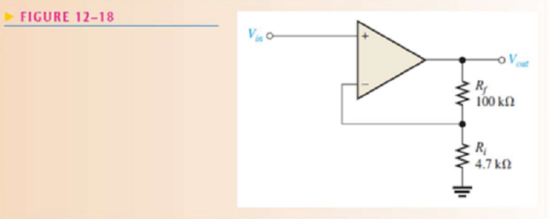
Determine the closed-loop voltage gain of the amplifier in Figure 12–18.
59.2
90.1
45.6
22.3
An infinite input impedance implies zero current at the inverting input. If there is zero current through the input impedance, then there must be no voltage drop between the inverting and noninverting inputs. Then, this means that
The voltage at the inverting (-) input is one because the noninverting (+) input is grounded
The voltage at the inverting (-) input is zero because the noninverting (+) input is grounded
The voltage at the inverting (-) input is one because the noninverting (+) output is grounded.
The voltage at the inverting (-) input is zero because the noninverting (+) output is grounded.
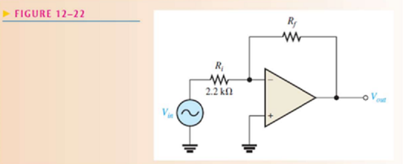
Given the op-amp configuration in Figure 12–22, determine the value of Rf required to produce a closed-loop voltage gain of -100.
220 Ω
22k Ω
220k Ω
A. 20k Ω
The op-amp voltage compares the magnitudes of two voltage inputs and determines which is the largest of the two
Comparator
Regulator
Integrator
Differentiator
A ________, also known as non-inverting comparator detects when an input voltage is above or more positive than the reference voltage.
Negative Voltage Comparator
Negative Voltage Comparator
Positive Voltage Comparator
Differentiator
A _________, also known as inverting comparator detects when an input voltage is below or more negative than the reference voltage
Negative Voltage Comparator
Window Comparator
Positive Voltage Comparator
Differentiator
The detects input voltage levels that are within a specific band or window of voltages, instead of indicating whether a voltage is greater or less than some preset or fixed voltage reference point.
Negative Voltage Comparator
Window Comparator
Positive Voltage Comparator
Differentiator
An operational amplifier is to be used with positive feedback to produce a Schmitt trigger circuit. If resistor, R1 = 40kΩ and resistor, R2 = 80kΩ, what will be the value of the width of the hysteresis if the op-amp is connected to a dual ±5v power supply
3.33 V
0 V
6.67 V
1.67 V
If the input to op-amp open loop comparator is a sinusoidal signal, then the output of the comparator is
Sine Wave
Cosine Wave
Rectangular Wave
Triangular Wave
Clamp diodes used in comparators ____
To protect the op-amp from damage
To develop the input offset current
To increase the output voltage
To increase the gain of op-amp
Introduction of hysteresis in a comparator makes it
A square waveform generator
Pulse generator
Immune to false triggering caused by noisy input signal
Prone to false triggering caused by noisy input signal
If the input signal varies rapidly or is not too noisy, operational amplifiers can be configured to operate as comparators in their ____.
Closed-loop mode
Open-loop mode
Steady mode
Both A and C
In the inverting configuration of comparator circuit, when VIN is greater than VREF, the op-amp comparators output will change state and saturate ___.
Towards the positive supply rail
Towards the negative supply rail
Back to the positive supply rail
None of the above
It is another type of operational amplifier circuit configuration that is used to combine the voltages present on two or more inputs into a single output voltage.
Differential Amplifier
Summing Amplifier
Integrating Amplifier
Instrumentation Amplifier
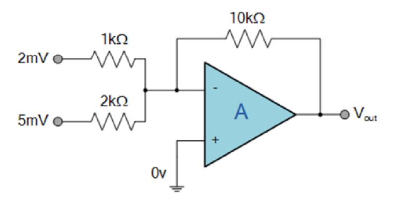
Find the output voltage of the following Summing Amplifier circuit.
45 mV
-45mV
-90 mV
90 mV
What is the formula for the Non-inverting Summing Amplifier Output Voltage?
Vout = ( V1 + V2 ) / 2
Vout = V1 + V2
Vout = 2 ( V1 + V2 )
Vout = [ 1 +RaRb ] [ V1+V22 ]
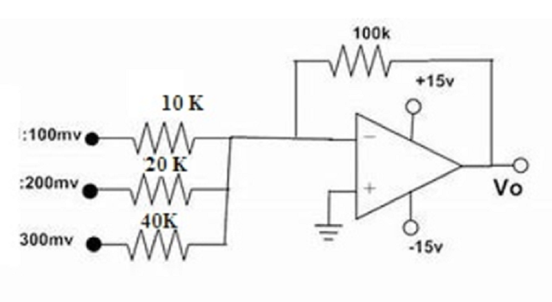
Find the output voltage of the following Summing Amplifier circuit.
2.75 V
-2.75 V
5.5V
-5.5 V
What is the basic application of the Summing Amplifier?
Digital to Analog Converter
Automatic Gain Control Circuit
Negative Feedback Circuit
Amplitude Modulation
Which of the following is the example of a basic schematic diagram of a Summing Amplifier?
0%
0
0%
0
0%
0
0%
0
What is the formula for the Non-inverting Summing Amplifier Output Voltage if Ra = Rb?
Vout = ( V1 + V2 ) / 2
Vout = V1 + V2
Vout = [ 1 +RaRb ] [ V1+V22 ]
Vout = 2 ( V1 + V2 )
If the inputs resistors, R1 , R2 , R3, etc. Are all equal a ___________ will be made.
Unity Gain Inverting Adder
Scaling Summing Amplifier
Non-inverting Summing Amplifier
Unity Gain Differential Amplifier
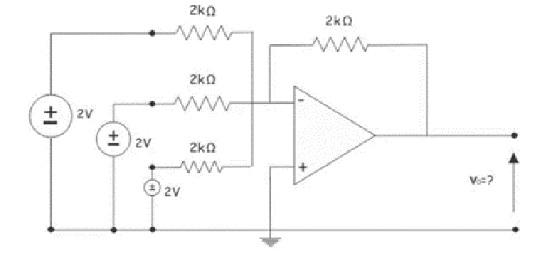
Find the output voltage of the following Summing Amplifier circuit.
6V
-6V
3V
-3V
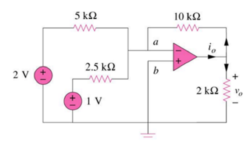
Find the output voltage of the following Summing Amplifier circuit
7.6 V
-7.6 V
3.8 V
-3.8V
The Miller Circuit is also known as
Non-Inverting Integrator
Inverting Integrator
Non-Inverting Differentiator
Inverting Differentiator
For an integrator, the slope of the frequency response is
Linear with negative slope
Linear with negative slope
Exponential increase
Exponential decrease
For the integration frequency, the expression is
CR
1/CR
R/C
C/R
For a differentiator, the frequency transfer function is
JωCR
-jωCR
1/jωCR
-1/jωCR
For a differentiator, the slope of the frequency response is
Linear with negative slope
Linear with positive slope
Exponential increase
Exponential decrease
The phase in the integrator and differentiator circuit respectively are
+90 degrees and +90 degrees
-90 degrees and -90 degrees
-90 degrees and +90 degrees
+90 degrees and -90 degrees
Consider a symmetrical square wave of 20-V peak-to-peak, 0 average, and 2-ms period applied to an inverting integrator. Determine the value of the time constant CR such that the triangular waveform at the output has a 20-V peak-to-peak amplitude.
0.25ms
0.50ms
2.5ms
5.0ms
The output of an RC differentiator is taken across the
Diode
Resistor
Capacitor
Transistor
For the differentiator time constant, the expression is
CR
1/CR
C/R
R/C
A circuit which produces a constant output voltage for a steadily changing input voltage is
Logic Circuit
Integrator circuit
Differentiator Circuit
Unilateral Circuit
{"name":"ELEX SYSTEM AND DESIGN-ECE3C", "url":"https://www.quiz-maker.com/QPREVIEW","txt":"Welcome to the ELEX System and Design Quiz, designed to test your knowledge and understanding of various electronic concepts. With 90 thought-provoking questions, this quiz challenges your grasp of MOSFETs, JFETs, biasing techniques, and transistor operations.Enhance your learning experience and see how well you can answer questions like:What determines the characteristics of MOSFETs?In which region of operation does the collector of a transistor act like a current source?How many terminals are there in a MOSFET?","img":"https:/images/course4.png"}
More Quizzes
ELECS COACHING VOLUME 3 PART 2
1015028
EI M-1
10512
GIVE AWAY STICKER 10 COIN
10511
Coach Quiz
1260
Quiz on Water Conservation - 15 Questions, Free Online
201015912
Fairy Tail - Prove Your Guild Mastery
201016612
Family Guy - How Well Do You Know the Show?
201018321
Which Yu-Gi-Oh Character Are You? Free Personality
201018709
Should I Be a Nurse? Free to See Your Fit
201017343
Gen Ed Practice Test - Free Mockboards
201016846
Pi - 300-Digit Memory Challenge
201016612
What Golf Driver Should I Buy? Free
201016612