Coaching ELEX 3
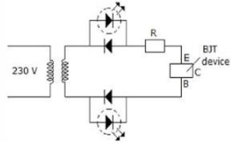
From the given circuit below, we can conclude that.
A. BJT is pnp
B. BJT is npn
C. Transistor is faulty
D. Not possible to determined
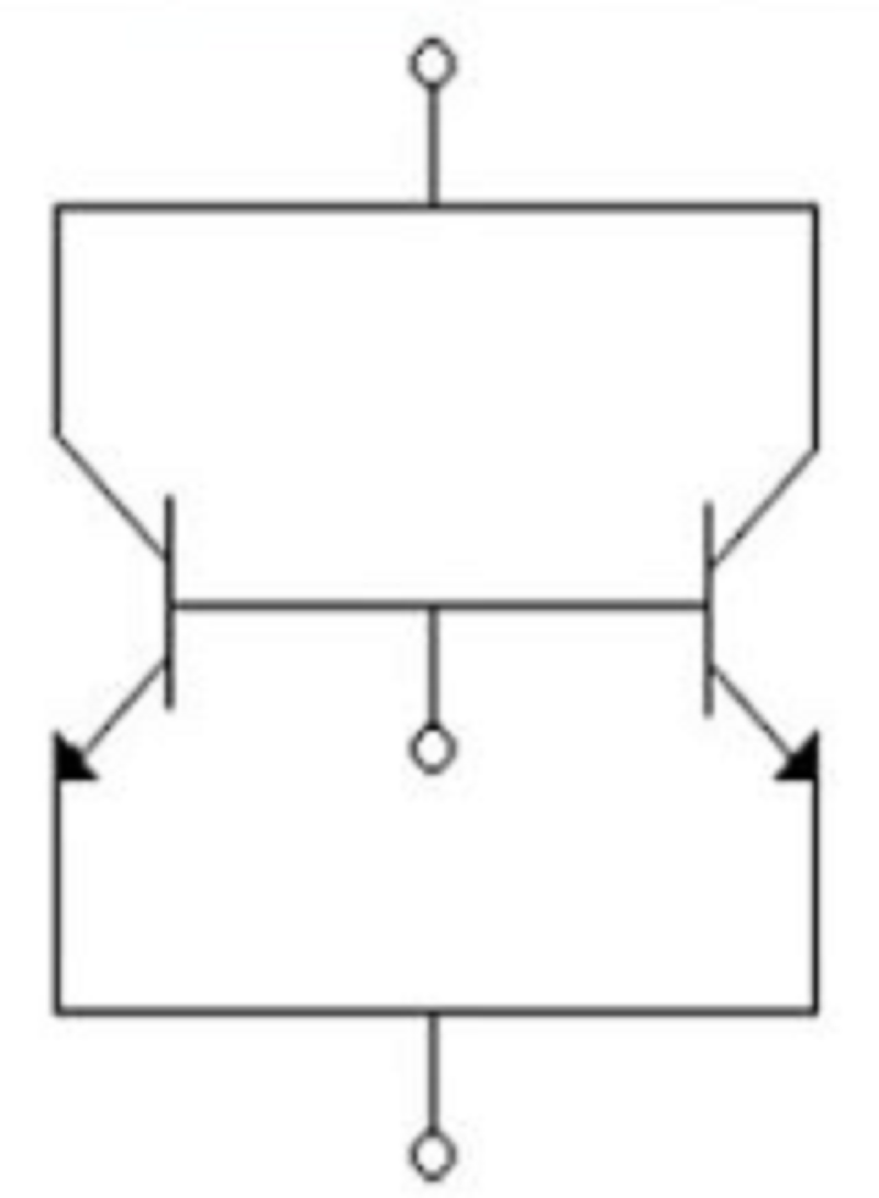
Discrete transistors T1 and T2 having maximum collector current rating of 0.75 amp are connected in parallel as shown in the figure, this combination is treated as a single transistor to carry a total current of 1 ampere, when biased with self bias circuit. When the circuit is switched on, T1 draws 0.55 amps and T2 draws 0.45 amps. If the supply is kept on continuously, ultimately it is very likely that
A. T1, and T2 get damaged
B. Both T1, and T2 will be safe.
C. T1 Will get damaged and T2 will be safe
D. T2 will get damaged and T1, will be safe.
In a piezoelectric crystal, applications of a mechanical stress would produce
A. Plastic deformation of the crystal
B. Magnetic dipoles in the crystal
C. Electrical polarization in the crystal
D. Shift in the Fermi level
In which of the following is the width of junction barrier very small?
A. Tunnel diode
B. Photo diode
C. PIN diode
D. Schottky diode
If the reverse voltage across a p-n junction is increased three times, the junction capacitance
A. Will decrease
B. Will increase
C. Will decrease by an approximate factor of about 2
D. Will increase by an approximate factor of about 2
Which of these has highly doped p and n region?
A. PIN diode
B. Tunnel diode
C. Schottky diode
D. Photodiode
Measurement of Hall coefficient enables the determination of
A. Recovery time of stored carrier
B. Type of conductivity and concentration of charge carriers
C. Temperature coefficient and thermal conductivity
D. Fermi level and forbidden energy gap
The units for transconductance are
A. Ohms
B. amperes
C. volts
D. siemens
The amount of photoelectric emission current depends on the frequency of incident light.
A. True
B. False
C. Lacks data
D. sometimes
When a p-n junction is forward biased
A. The width of depletion layer increases
B. The width of depletion layer decreases
C. The majority carriers move away from the junction
D. The current is very small
The carriers of n channel JFET are
A. Free electrons and holes
B. holes
C. Free electrons or holes
D. Free electrons
The depletion layer around p-n junction in JFET consists of
A. hole
B. electron
C. Immobile charges
D. None of the above
Junction temperature is always the same as room temperature.
A. True
B. False
C. Lacks data
D. sometimes
The mean free path of conduction electrons in copper is about 4 x 10⁻⁸ m. For a copper block, find the electric field which can give, on an average, 1 eV energy to a conduction electron
A. 2.62 x 10⁷ V/m
B. 2.64 x 10⁷ V/m
C. 2.5 x 10⁷ V/m
D. 2.58 x 10⁷ V/m
When a p-n-p transistor is properly biased to operate in active region the holes from emitter.
A. Diffuse through base into collector region
B. Recombine with electrons in base
C. Recombine with electrons in emitter
D. None of the above
Assertion (A): Silicon is preferred over germanium in manufacture of semiconductor devices.
Reason (R): Forbidden gap in silicon is more than that in germanium.
A. Both A and R are true and R is correct explanation of A
B. Both A and R are true but R is not a correct explanation of A
C. A is true but R is false
D. A is false but R is true
Assertion (A): A decrease in temperature increases the reverse saturation current in a p-n diode.
Reason (R): When a diode is reverse biased surface leakage current flows.
A. Both A and R are true and R is correct explanation of A
B. Both A and R are true but R is not a correct explanation of A
C. A is true but R is false
D. A is false but R is true
At room temperature a semiconductor material is
A. Perfect insulator
B. conductor
C. Slightly conducting
D. Any of the above
The static characteristic of an adequately forward biased P-n junction is a straight line, if the plot is of __________ Vs → versus
A. log I Vs log V
B. log I Vs V
C. I Vs log V
D. I Vs V
In an n channel JFET
A. ID, IS and IG are considered positive when flowing into the transistor
B. ID and IS are considered positive when flowing into transistor and IG is considered positive when flowing out of it
C. ID, IS, IG are considered positive when flowing out of transistor
D. IS and IG are considered positive when flowing into transistor and ID is considered positive when flowing out of it
The intrinsic carrier concentration of silicon sample at 300 K is 1.5 x 10^16/m3. If after doping, the number of majority carriers is 5 x 10^20/m3. The minority carrier density is
A. 4.5 x 10^11/m3
B. 3.33 x 10^4/m3
C. 5 x 10^20/m3
D. 3 x 10^-5/m3
A diode is operating in forward region and the forward voltage and current are v = 3 + 0.3 sin ωt (volts) and I = 5 + 0.2 sin ωt (mA). The average power dissipated is
A. 15 mW
B. about 15 mW
C. 1.5 mW
C. about 1.5 mW
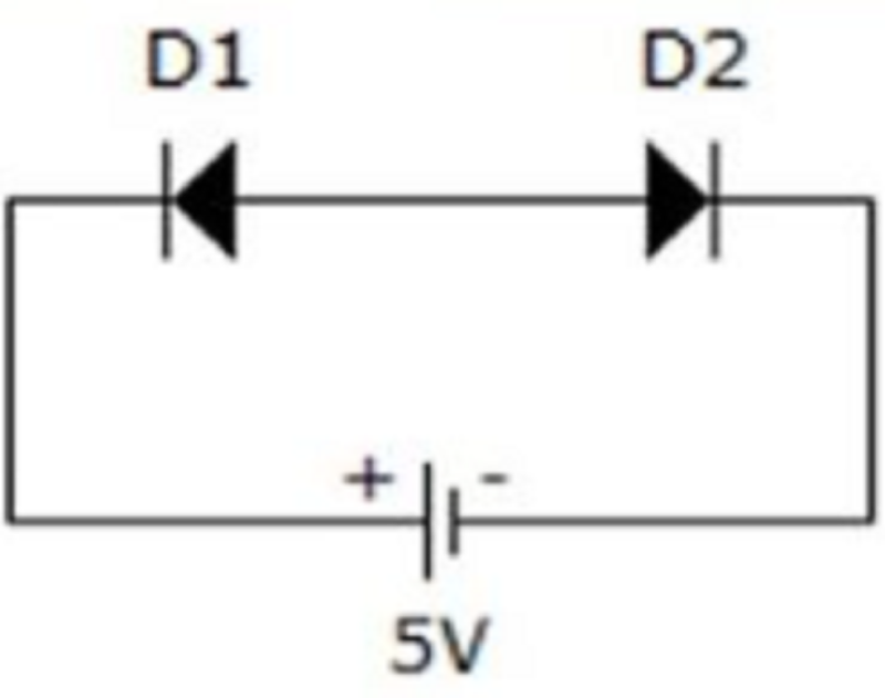
Two identical silicon diodes D1 and D2 are connected back to back shown in figure. The reverse saturation current Is of each diode is 10-8 amps and the breakdown voltage VBr is 50 v. Evaluate the voltages VD1 and VD2 dropped across the diodes D1 and D2 assuming KT/q to be 25 m V.
A. 4.983 V, 0.017 V
B. - 4.98 V, - 0.017 V
C. 0.17 V, 4.983 V
D. - 0.017 V, - 4.98 V
For BJT transistor. The maximum power dissipation is specified as 350 mW if ambient temperature is 25°C. If ambient temperature is 60°C the maximum power dissipation should be limited to about
A. 100 mW
B. 250 mW
C. 450 mW
D. 600 mW
The concentration of minority carriers in a semiconductor depends mainly on
A. The extent of doping
B. temperature
C. The applied bias
D. None of the above
Which of the following has highest conductivity?
A. Silver
B. Aluminium
C. Tungsten
D. Platinum
In a bipolar junction transistor the base region is made very thin so that
A. Recombination in base region is minimum
B. Electric field gradient in base is high
C. Base can be easily fabricated
D. Base can be easily biased
Compared to bipolar junction transistor, a JFET has
A. Lower input impedance
B. High input impedance and high voltage gain
C. Higher voltage gain
D. High input impedance and low voltage gain
The drain characteristics of JFET in operating region, are
A. Inclined upwards
B. Almost flat
C. Inclined downwards
D. Inclined upwards or downwards
As temperature increases
A. The forbidden energy gap in silicon and germanium increase
B. The forbidden energy gap in silicon and germanium decrease
C. The forbidden energy gap in silicon decreases while that in germanium decreases
D. The forbidden energy gap in silicon increases while that in germanium decreases
When a reverse bias is applied to a p-n junction, the width of depletion layer.
A. decreases
B. increases
C. Remains the same
D. May increase or decrease
The Hall constant in Si bar is given by 5 x 103 cm3/ coulomb, the hole concentration in the bar is given by
A. 10^5/cm3
B. 1.25 x 10^15/cm3
C. 1.5 x 10^15/cm3
D. 1.6 x 10^15/cm3
Which of the following devices has a silicon dioxide layer?
A. NPN transistor
B. Tunnel diode
C. JFET
D. MOSFET
Which statement is false as regards holes
A. Holes exist in conductors as well as semiconductors
B. Holes constitute positive charges
C. Holes exist only in semiconductors
D. Holes and electrons recombine
Photo electric emission can occur only if
A. Wave length of incident radiation is equal to threshold value
B. Wave length of incident radiation is less than threshold value
C. Frequency of incident radiation is less than threshold frequency
D. None of the above
The reverse saturation current of a diode does not depend on temperature.
A. True
B. False
C. Lacks data
D. sometimes
The value of α in a transistor
A. Is always equal to 1
B. Is less than 1 but more than 0.9
C. Is about 0.4
D. Is about 0.1
At room temperature the current in an intrinsic semiconductor is due to
A. holes
B. electrons
C. ions
D. Holes and electrons
Work function is the maximum energy required by the fastest electron at 0 K to escape from the metal surface.
A. True
B. False
C. Lacks data
D. sometimes
The most commonly used semiconductor material is
A. silicon
B. germanium
C. Mixture of silicon and germanium
D. None of the above
In which of these is reverse recovery time nearly zero?
A. Zener diode
B. Tunnel diode
C. Schottky diode
D. PIN diode
A transistor has a current gain of 0.99 in the CB mode. Its current gain in the CC mode is
A. 100
B. 99
C. 1.01
D. 0.99
In p-n-p transistor the current IE has two components viz. IEP due to injection of holes from p-region to n-region and IE due to injection of electrons from n-region to p-region. Then
A. IEp and IEn are almost equal
B. IEp >> IEn
C. IEn >> IEp
D. either (a) or (c)
In an n channel JFET, the gate is
A. N type
B. P type
C. Either n or p
D. Partially n & partially p
The amount of photoelectric emission current depends on
A. Frequency of incident radiation
B. Intensity of incident radiation
C. Both frequency and intensity of incident radiation
D. None of the above
Assertion (A): A p-n junction has high resistance in reverse direction.
Reason (R): When a reverse bias is applied to p-n junction, the width of depletion layer increases.
A. Both A and R are true and R is correct explanation of A
B. Both A and R are true but R is not a correct explanation of A
C. A is true but R is false
D. A is false but R is true
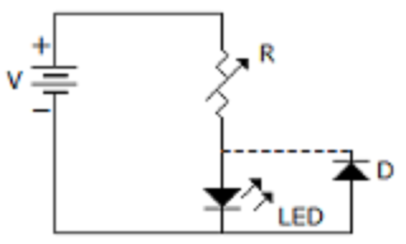
In the circuit of figure the function of resistor R and diode D are
A. To limit the current and to protect LED against over voltage
B. To limit the voltage and to protect LED against over current
C. To limit the current and protect LED against reverse breakdown voltage.
D. None of the above.
At very high temperatures the extrinsic semi-conductors become intrinsic because
A. Drive in diffusion of dopants and carriers
B. Band to band transition dominants over impurity ionization
C. Impurity ionization dominants over band to band transition
D. Band to band transition is balanced by impurity ionization
When a voltage is applied to a semiconductor crystal then the free electrons will flow.
A. Towards positive terminal
B. Towards negative terminal
C. Either towards positive terminal or negative terminal
D. Towards positive terminal for 1 μs and towards negative terminal for next 1 μs
Ferrite have
A. Low copper loss
B. Low eddy current loss
C. Low resistivity
D. Higher specific gravity compared to iron
In a p type material the Fermi level is 0.3 eV above valence band. The concentration of acceptor atoms is increased. The new position of Fermi level is likely to be
A. 0.5 eV above valence band
B. 0.28 eV above valence band
C. 0.1 eV above valence band
D. Below the valence band
In an n-p-n transistor, the majority carriers in the base are
A. electrons
B. holes
C. Both holes and electrons
D. Either holes or electrons
An LED has a rating of 2 V and 10 mA. It is used along with 6V battery. The range of series resistance is
A. 0 to 200 Ω
B. 200 - 400 Ω
C. 200 Ω and above
D. 400 Ω and above
The number of doped regions in PIN diode is
A. 1
B. 2
C. 3
D. 1 or 2
A transistor has two p-n junctions. The batteries should be connected such that
A. Both junctions are forward biased
B. Both junctions are reverse biased
C. One junction is forward biased and the other is reverse biased
D. None of the above
In a bipolar transistor the barrier potential
A. 0
B. A total of 0.7 V
C. 0.7 V across each depletion layer
D. 0.35 V
Recombination produces new electron-hole pairs
A. True
B. False
C. Lacks data
D. sometimes
As compared to an ordinary semiconductor diode, a Schottky diode
A. Has lower cut in voltage
B. Has higher cut in voltage
C. Lower reverse saturation current
D. both (b) and (c)
Assertion (A): When a high reverse voltage is applied to a p-n junction the diode breaks down.
Reason (R): High reverse voltage causes Avalanche effect.
A. Both A and R are true and R is correct explanation of A
B. Both A and R are true but R is not a correct explanation of A
C. A is true but R is false
D. A is false but R is true
As compared to an ordinary semiconductor diode, a Schottky diode
A. Has higher reverse saturation current
B. Has higher reverse saturation current and higher cut in voltage
C. Has higher reverse saturation current and lower cut in voltage
D. Has lower reverse saturation current and lower cut in voltage
Crossover distortion behaviour is characteristic of
A. class A O/P stage
B. class B O/P stage
C. class AB output stage
D. Common pulse O/P state
If αac for transistor is 0.98 then βac is equal to
A. 51
B. 49
C. 47
D. 45
Assertion (A): The conductivity of p type semiconductor is higher than that of intrinsic semiconductor.
Reason (R): The addition of donor impurity creates additional energy levels below conduction band.
A. Both A and R are true and R is correct explanation of A
B. Both A and R are true but R is not a correct explanation of A
C. A is true but R is false
D. A is false but R is true
In an n-p-n transistor biased for operation in forward active region
A. Emitter is positive with respect to base
B. Collector is positive with respect to base
C. Base is positive with respect to emitter and collector is positive with respect to base
D. None of the above
An increase in temperature increases the width of depletion layer.
A. True
B. False
C. Lacks data
D. sometimes
A zener diode is used in
A zener diode is used in
B. Amplifier circuits
C. Both voltage regulator and amplifier circuit
D. None of the above
A particular green LED emits light of wavelength 5490, Å, the energy bandgap of the semiconductor material used there is .. h = 6.6 x 10^-34 J sec.
A. 2.26 eV
B. 1.98 eV
C. 1.17 eV
D. 0.74 eV
In a zener diode
A. The forward current is very high
B. Sharp breakdown occurs at a certain reverse voltage
C. The ratio v-i can be negative
D. There are two p-n junctions
In a bipolar transistor which current is largest
A. Collector current
B. Base current
C. Emitter current
D. Base current or emitter current
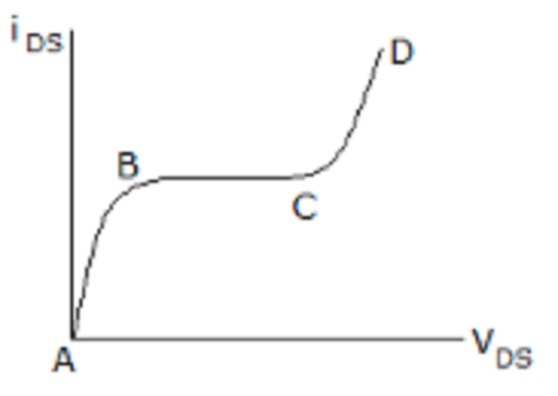
The v-i characteristics of a FET is shown in figure. In which region is the device biased for small signal amplification
A. AB
B. BC
C.CD
D.BD
Secondary emission is always decremental.
A. True
B. False
C. Lacks data
D. sometimes
In a degenerate n type semiconductor material, the Fermi level,
A. Is in valence band
B. Is in conduction band
C. Is at the centre in between valence and conduction bands
D. Is very near valence band
The types of carriers in a semiconductor are
A. 1
B. 2
C. 3
D. 4
A potential of 7 V is applied to a silicon diode. A resistance of 1 Kohm is also in series with the diode. The current is
A. 7 mA
B. 6.3 mA
C. 0.7 mA
D. 0
Assertion (A): The reverse saturation current in a semiconductor diode is 4nA at 20°C and 32 nA at 50°C.
Reason (R): The reverse saturation current in a semiconductor diode doubles for every 10°C rise in temperature.
A. Both A and R are true and R is correct explanation of A
B. Both A and R are true but R is not a correct explanation of A
C. A is true but R is false
D. A is false but R is true
Calculate the stability factor and change in IC from 25°C to 100°C for, β = 50, RB/ RE = 250, ΔIC0 = 19.9 nA for emitter bias configuration.
A. 42.53, 0.85 μA
B. 40.91, 0.58 μA
C. 40.91, 0.58 μA
D. 41.10, 0.39 μA
The center frequency of a band-pass filter is always equal to the
A. bandwidth
B. –3 dB frequency
C. Bandwidth divided by Q
D. Geometric average of the critical frequencies
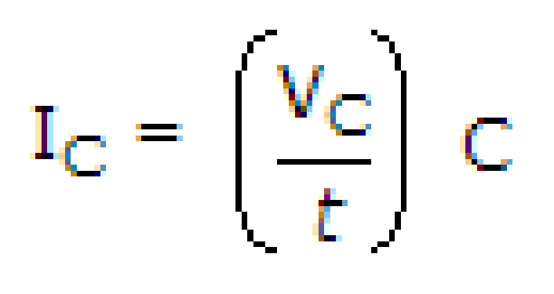
The formula shows that for a given capacitor, if the voltage changes at a constant rate with respect to time, the current will
A. increase
B. decrease
C. Be constant
D. Decrease logarithmically
A zero-level detector is a
A. Comparator with a sine-wave output
B. Comparator with a trip point referenced to zero
C. Peak detector
D. limiter
A digital-to-analog converter is an application of the
A. Scaling adder
B. voltage-to-current converter
C. Noninverting amplifier
D. Adjustable bandwidth circuit
If the value of resistor Rf in an averaging amplifier circuit is equal to the value of one input resistor divided by the number of inputs, the output will be equal to
A. The average of the individual inputs
B. The inverted sum of the individual inputs
C. The sum of the individual inputs
D. The inverted average of the individual inputs
If the input to a comparator is a sine wave, the output is a
A. Ramp voltage
B. Sine wave
C. Rectangular wave
D. Sawtooth wave
A basic series regulator has
A. An error detector
B. A load
C. A reference voltage
D. Both an error detector and a reference voltage
A comparator is an example of a(n)
A. Active filter
B. Current source
C. Linear circuit
D. Nonlinear circuit
Initially, the closed-loop gain (Acl) of a Wien-bridge oscillator should be
A. Acl < 3
B. Acl > 3
C. 0
D. Acl =1
In an averaging amplifier, the input resistances are
A. Equal to the feedback resistance
B. Less than the feedback resistance
C. Greater than the feedback resistance
D. unequal
A triangular-wave oscillator can consist of an op-amp comparator, followed by a(n)
A. differentiator
B. amplifier
C. integrator
D. multivibrator
The ramp voltage at the output of an op-amp integrator
A. Increases or decreases at a linear rate
B. Increases or decreases exponentially
C. Is always increasing and never decreasing
D. Is constant
A two-pole high-pass active filter would have a roll-off rate of
A. 40 dB/decade
B. –40 dB/decade
C. 20 dB/decade
D. –20 dB/decade
The product kT (where k is Boltzmann's constant and T is absolute temperature) at room temperature is about
A. 0.051 eV
B. 0.026 eV
C. 0.01 eV
D. 0.001 eV
If E is energy level of electron and EF is fermi level, and T = 0 and E > EF, then
A. The probability of finding an occupied quantum state of energy higher than EF is zero
B. All quantum states with energies greater than EF are occupied
C. Some quantum states with energies greater than EF are occupied
D. Majority of quantum states with energies greater than EF are occupied
Which variety of copper has the best conductivity?
A. Pure annealed copper
B. Hard drawn copper
C. Induction hardened copper
D. Copper containing traces of silicon
The number of valence electrons in a silicon atom is
A. 4
B. 2
C. 1
D. 0
In a JFET VDS exceeds the rated value. Then it operates in
A. Active region
B. Ohmic region
C. Cut off region
D. Either cut off or active region

Figure represents a
A. Diode rectifier
B. Schottky diode
C. Varistor
D. None of the above
The output, V-I characteristics of an Enhancement type MOSFET has
A. Only an ohmic region
B. Only a saturation region
C. An ohmic region at low voltage value followed by a saturation region at higher voltages
D. An ohmic region at large voltage values preceded by a saturation region at lower voltages
Piezoelectric quartz crystal resonators find application where
A. Signal amplification is required
B. Rectification of the signal is required
C. Signal frequency control is required
D. Modulation of signal is required
The forbidden energy gap between the valence band and conduction band will be least in case of
A. metals
B. semiconductors
C. insulators
D. All of the above
If too large current passes through the diode
A. All electrons will leave
B. All holes will freeze
C. Excessive heat may damage the diode
D. Diode will emit light
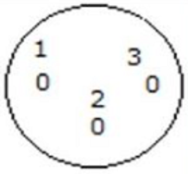
Figure shows the terminals of a transistor in plastic package TO 18. Then
A. terminals 1, 2, 3 are emitter, collector, base respectively
B. terminals 1, 2, 3 are emitter, base, collector respectively
C. terminals 1, 2, 3 are base, emitter collector, respectively
D. terminals 1, 2, 3 are collector, emitter, base respectively
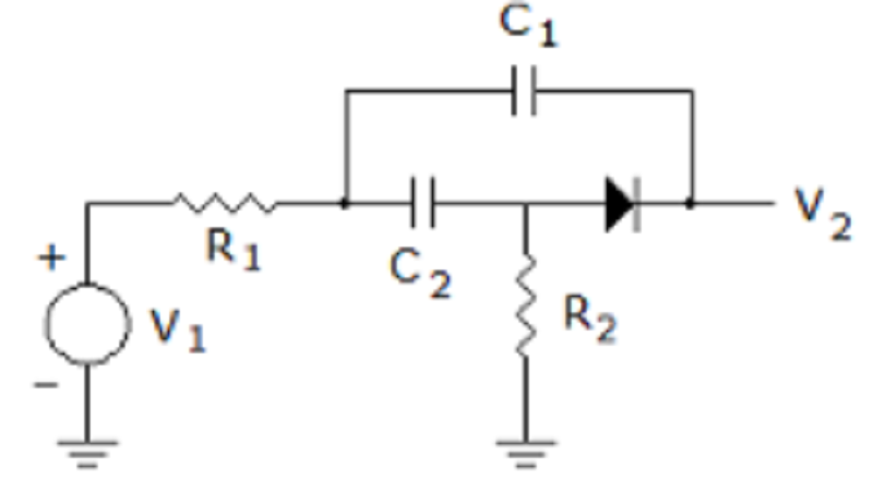
The network shown in the figure represents a
A. Band pass filter
B. Low pass filter
C. High pass filter
D. Band stop filter
In a bipolar transistor, the emitter base junction has
A. Forward bias
B. Reverse bias
C. Zero bias
D. Zero or reverse bias
Which of these has semi-conductor metal junction?
A. PIN diode
B. Photo diode
C. Tunnel diode
D. Schottky diode
The ripple factor of power supply is a measure of
A. Its filter efficiency
B. Diode rating
C. Its voltage regulation
D. Purity of power output
{"name":"Coaching ELEX 3", "url":"https://www.quiz-maker.com/QPREVIEW","txt":"From the given circuit below, we can conclude that., Discrete transistors T1 and T2 having maximum collector current rating of 0.75 amp are connected in parallel as shown in the figure, this combination is treated as a single transistor to carry a total current of 1 ampere, when biased with self bias circuit. When the circuit is switched on, T1 draws 0.55 amps and T2 draws 0.45 amps. If the supply is kept on continuously, ultimately it is very likely that, In a piezoelectric crystal, applications of a mechanical stress would produce","img":"https://www.quiz-maker.com/3012/CDN/87-4239898/338506804-5457576174343565-8011852385976828539-n.png?sz=1200"}
More Quizzes
CNA
1160
Quiz με διάσημα αποφθέγματα
1050
Grade X
20100
Do you have any recommendations in new papers today?
100
What Stranger Things Character Are You? Free
201018760
PKU NCLEX Practice - What's True of PKU?
201020484
BLACKPINK's Jisoo: What Is Her Favorite Color?
201023541
Marching Band: Procedures & Field Protocols
15815315
Why Am I Sad - Free Mood Self-Assessment Online
201018680
Cytology with Answers - Free Interpretive Cases
15817786
Am I Fun to Hang Out With? to Take With Friends
201017856
¿Qué personaje de Steven Universe eres? - Test gratis
201018445