
PCM Modulation Quiz

PCM Modulation Quiz
Test your knowledge on Pulse Code Modulation (PCM) with this comprehensive quiz. From the basics of digital signal conversion to advanced modulation techniques, this quiz covers various topics that are essential for understanding PCM.
- Explore the basics of PCM coding
- Discover the advantages of digital signals
- Learn about the components of a PCM modulator
PCM modulation is a kind of ------ coding
binary
octal
source
hexadecimal
The meaning of ----- coding is the conversion from analog signal to digital signal
octal
source
hexadecimal
binary
After converted to ------ signal, it is easy for us to process the signal such as encoding, filtering the unwanted signal
analog
binary
octal
digital
In communications systems, the quality of ----- signal is better than analog signal.
digital
binary
octal
good analog
In PCM system, the digital signal can be easily ------ by using comparator.
found
filtered
recovered
determined
In PCM modulation is commonly used in ------- and telephone transmission.
analog
digital
video
audio
The main advantage is the PCM modulation only needs ------ sampling frequency
4 kHz
8 kHz
6 kHz
2 kHz
In PCM modulator, the low-pass filter is used to remove the ------ in the audio signal.
low frequency
high frequency
noise
unwanted
In PCM modulator, the audio signal will be ------ to obtain a series of sampling values.
sampled
encoded
decoded
selected
In PCM modulator, the signal will pass through ------- to quantize the sampling values.
a sampler
a LPF
an encoder
a quantizer
In PCM modulator, signal will pas through ------- to encode the quantization values
a decoder
an encoder
a sampler
a quantizer
In PCM modulator, the process of quantization can be achieved at one time by ----converter.
DCA
DAC
ACD
ADC
If the bits for PCM modulation is 3, then the quantization levels is ----
8
16
4
12
If the bits for PCM modulation is 4, then the quantization levels is ----
12
8
16
4
The increasing of bits of PCM modulation will prevent the signal from -----
detailed
noise
unwanted
distortion
The increasing of bits of PCM modulation will ------- the bandwidth.
increase
decrease
enhance
destroyed
In PCM modulator, we need to convert the ----- data to serial data, to satisfy the data format of PCM modulation.
analog
digital
parallel
binary
In PCM modulator, we need to convert the parallel data to ------ data, to satisfy the data format of PCM modulation
series
parallel
diagonal
serial
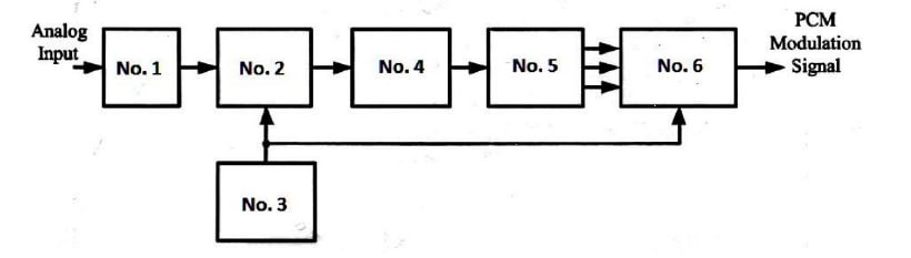
In Figure (1), the name of the box no. 1 is -------
quantizer
sampler
LPF
encoder
In Figure (1), the name of the box no. 2 is --------------.
sampler
LPF
quantizer
encoder
In Figure (1), the name of the box no. 3 is --------------
encoder
LPF
sampler
clock
In Figure (1), the name of the box no. 4 is --------------
quantizer
encoder
LPF
sampler
In Figure (1), the name of the box no. 6 is --------------
LPF
quantizer
parallel to serial converter
encoder
In Figure (1), the name of the box no. 5 is --------------
LPF
quantizer
parallel to serial converter
encoder
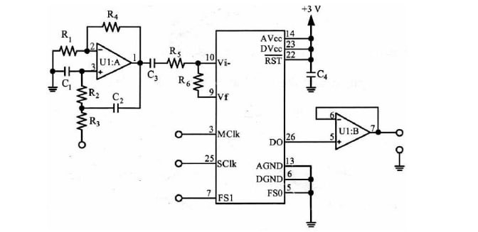
In the circuit shown in Figure (2), capacitors C1, C2, resistors R1, R2, R3, R4, and µA741comprise a ------
encoder
sampler
low-pass filter
quantizer
In the circuit shown in Figure (2), the voltage gain of the low pass filter is ------
1+R1/R4
1+R4/R1
1+R3/R2
1+R2/R3
In the circuit shown in Figure(2), if R2 = R3 = R and C1 = C2 = C, the cutoff frequency fo is equal to -------
R/(2p C)
2p/(RC)
2p (R/C)
1/(2pRC)
The circuit shown in Figure (2) is used to implement -------- modulator.
ASK
PCM
FSK
PSK
In the circuit shown in Figure (2), the ------ signal will pass through R5, and input to pin 10, which is the inverting input terminal.
analog
digital
sampled
received
In the circuit shown in Figure (2), master clock is the operation frequency of the system, which is ------- square wave frequency.
2048 Hz
2048 MHz
2048 kHz
4096 MHz
In the circuit shown in Figure (2), master clock of the system has a shape of ------- wave form.
square
triangular
sawtooth
sinusoidal
In the circuit shown in Figure (2), the sampling frequency is ------
12 KHz
8 KHz
4 KHz
10 KHz
In the circuit shown in Figure (2), the sampler will sample the input audio signal in every -
0.1 ms
83 µs
0.125 ms.
25 ms
In the circuit shown in Figure (2), the sampling frequency is obtained by using the counter to divide the master clock frequency by -----
64
128
512
256
In the circuit shown in Figure (2), when FS0 = 0 and FS1 = 0, the output format is ------
8 bits CVSD
16-bits Linear
8-bits µ-Law
8-bits A-Law
In the circuit shown in Figure (2), when FS0 = 0 and FS1 = 1, the output format is ------
8-bits A-Law
8 bits CVSD
8-bits A-Law
16-bits Linear
In the circuit shown in Figure (2), when FS0 = 1 and FS1 = 0, the output format is ------
8-bits A-Law
8-bits µ-Law
8 bits CVSD
16-bits Linear
In the circuit shown in Figure (1), when FS0 = 1 and FS1 = 1, the output format is ------
8-bits µ-Law
16-bits Linear
8 bits CVSD
8-bits A-Law
In early days, the communication system is mostly using the ----- signal to transmit signals.
analog or digital
digital
analog
analog and digital
Due to the ------ network communications, a lot of data or information is transmitted by using the technique of pulse wave modulation.
analog
digital
analog or digital
analog and digital
Pulse wave modulation can be used to transmit the ------ signal or data with a certain rate.
digital audio
analog video
digital video
analog audio
PAM, PWM and PPM modulations belong to ------ modulation
analog
digital
analog and digital
analog or digital
PCM modulations belong to ------ modulation.
analog
digital
analog and digital
analog or digital
The PCM modulation is a real ------ signal that can be processed and stored by computer.
analog or digital
analog and digital
analog
digital
For any pulse wave modulation, before modulating, the original continuous type signal must be ------
encoded
sampled
quantized
stored
The sampling rate of the sampling signal cannot be -----, or else the recovered signal will cause distortion
very high
moderate
too high
too low
If the sampling rate excesses double or more times of the maximum frequency of the signal, then the distortion level of the data recovery at the receiver will be the ------.
minimum
maximum
bad
good
If the frequency range of the audio signal is 40 Hz to 4 kHz, then the sampling signal frequency of the pulse wave modulation must be at least ------
4 kHz
12 KHz
8 kHz
10 kHz
Before the PCM signal sends into the PCM demodulator, we utilize a----- to recover the signal to the original level.
quantizer
encoder
LPF
comparator
Before demodulating PCM, the pulse wave signal will be converted to ----- digital signal.
serial
serial or parallel
parallel
serial and parallel
In the block diagram shown in Figure (1), the box no. 1 is called ------
S/H
decoder
comparator
LPF
In the block diagram shown in Figure (1), the box no. 2 is called ------
decoder
clock
S/H
encoder
In the block diagram shown in Figure (1), the box no. 3 is called ------
clock
LPF
decoder
S to P converter
In the block diagram shown in Figure (1), the box no. 4 is called ------
decode
comparator
S/H
clock
In the block diagram shown in Figure (1), the box no. 5 is called ------
S to P converter
decode
S/H
LPF
In the block diagram shown in Figure (1), the box no. 6 is called ------
S/H
LPF
decode
comparator
In PCM demodulator, the decoder will be n-bit ------
DAC
ADC
DCA
ACD
In PCM demodulator, we utilize a ----- to remove the unwanted signal at the final part
HPF
BPF
LPF
digital filter
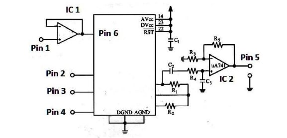
The circuit diagram shown in Figure (2) is called ------ demodulator.
ASK
PCM
FSK
PSK
In the circuit diagram shown in Figure (2), the fun
LPF
positive amplifier
inverted amplifier
buffer
In the circuit diagram shown in Figure (2), its input at ------
Pin 1
Pin 2
Pin 3
Pin 4
In the circuit diagram shown in Figure (2), the master clock is connected to -----
Pin 1
Pin 2
Pin 4
Pin 5
In the circuit diagram shown in Figure (2), the value of its master clock is ----- kHz
512
1024
4069
2048
In the circuit diagram shown in Figure (2), the sample clock is connected to -----
Pin 1
Pin 2
Pin 3
Pin 4
In the circuit diagram shown in Figure (2), the value of its sample clock is ----- kHz
8
4
16
2
In the circuit diagram shown in Figure (2), the encode mode selection is connected to -----
Pin 5
Pin 4
Pin 3
Pin 2
In the circuit diagram shown in Figure (2), the output signal is taken from -----
Pin 6
Pin 3
Pin 5
Pin 4
In the circuit diagram shown in Figure (2), the input modulated signal is connected to ------
Pin 5
Pin 6
Pin 4
Pin 3
From Figure (2), capacitor C3, resistors R3, R4, R5, and IC2 comprise a first order active ---
BPF
HPF
matched filter
LPF
In the circuit diagram shown in Figure (2), the gain of IC2 is given by:
–R5/R3
–R3/R5
–R5/R4
R4/R5
In the circuit diagram shown in Figure (2), the cutoff frequency of IC2 is given by:
1/(2pR4C3)
1/(2pR5C3)
1/(2pR3C3)
1/(2pR3C2)
{"name":"PCM Modulation Quiz", "url":"https://www.quiz-maker.com/QPREVIEW","txt":"Test your knowledge on Pulse Code Modulation (PCM) with this comprehensive quiz. From the basics of digital signal conversion to advanced modulation techniques, this quiz covers various topics that are essential for understanding PCM.Explore the basics of PCM codingDiscover the advantages of digital signalsLearn about the components of a PCM modulator","img":"https:/images/course8.png"}